

SIM-image 3D reconstruction analysis service
(Observation service for sectional structure / failure analysis)
- Empty
- Empty
- Empty
Failure analysis of semiconductor devices and observation of work cross section / laminated structure with high accuracy and high resolution
The focused ion beam (FIB) processing device can perform slicing at very small equi-interval pitches, as well as the ability to acquire images each time.By using this function,With high-precision exposure of workpiece cross section and high resolution image acquisition,Observation of cross sectional shape and laminated structure can be done as analysis of defects of minute workpieces.For example, it enables failure analysis of semiconductor devices, observation of cross-sectional shape of wire bond, confirmation of laminated structure of plating and thickness.
※ If you wish not only observation but also analysis service,
We are introducing contract analysis of Toray Research Center Co., Ltd.
Please feel free to contact us.
Features
- Creates data reconstructed from sequential machinings and observations
- Slice data is superimposed to create high-precision, high-quality 3D data
- Slice pitch can be adjusted from 1 nm to 1 µm
- High-resolution SIM image observation
- Observation target: Up to 200 μm side can be supported
- It is possible to observe microscopic observation objects that disappears in polishing processing
Method
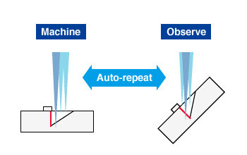
- Cross-sectional slice machining and observation is repeated at set intervals to obtain multiple cross-section SIM images and build a 3D reconstruction
- Machined surface is observed at a near-perpendicular angle, creating reconstructed data from high-quality images
Analysis example
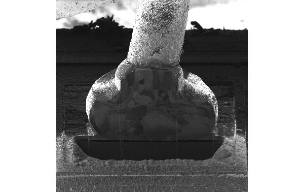
【Sample】 Au wire bonding part of optical sensor
【Size】 ・width 100µm ・high 100µm ・pitch 0.5μm
Observation movie of Au wire bonding part of optical sensor
Application example
- Observation for failure analysis of power semiconductors
- Observation of cross-sectional shape of wire bonding part
- Laminate structure of plating · Thickness observation, etc.