

Focused ion beam (FIB) machining

- Empty
- Empty
- Empty
Nano-order machining at ⌀1 micron or less
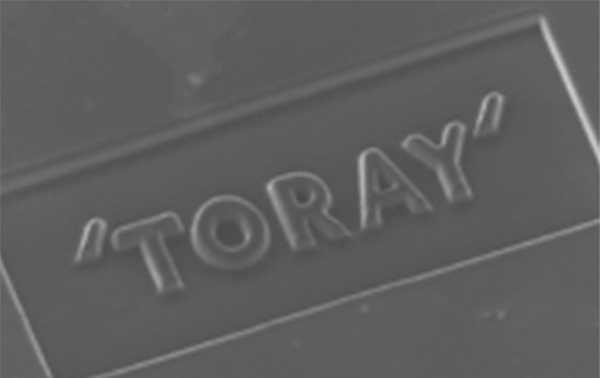
This method machines material by smashing ions against it, knocking atoms off of the surface. This provides a broader range of machining sizes, from several microns wide to nano-order work. Work can also be done at extremely low speeds and voltages for low-damage machining.
Features
Allows for high-speed, large-area machining with a high probe current. Secondary electron imaging resolution: 5 nm or less
Maskless machining is possible, allowing for selective etching only in the range exposed to the beam. This eliminates the mask creation process, cutting costs.
3D reconstruction analysis lets you observe the process and state of machining with the FIB device. This lets operators solve issues that occur during machining.
 φ0.5µm multi-hole machining(SUS t2µm)
 φ5µm machining(SUS t5µm)
 Micro-machining on tools (ZrO2)
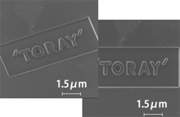 Micro-machining(Si)
Chief machining specs
| Maximum work size | 50(X)×50(Y)×10(Z)mm |
|---|---|
| Minimum machined size (guide) | Groove width: 100 nm (~L/D=3), hole diameter: ⌀200 nm (~L/D=5) |
| Minimum machined hole diameter | φ0.5μm |
| Aspect radio | Approx. 5-6x |
| Target material | Metals, ceramics |